PCB Via

An In-Depth Guide to PCB Vias and PCB Design

Guy Shemesh | 15/9/2021

Introduction

PCB vias are fundamentally important in PCB design, it is important to understand this topic in detail because proper via design is key for a reliable PCB that is both cost-effective and can be produced with high yield.

Vias and layer interconnect are the number one priority of the manufacturer. The manufacturer will inspect your vias prior to fabrication and may make changes to your original design if it does not meet his tolerances - many times without you even knowing about it! The manufacturer can change the drilled hole, annular ring, and the clearances around them. However, the manufacturer has limited freedom because he is constrained by the original design. Changing the original design as an afterthought just before fabrication is never a good idea, it is always better to design proper vias during the layout of the board and submit correct Gerber files to the factory.

This guide is based on our 15+ years of knowledge in the PCB design industry. It is believed to be accurate and up to date with the current fabrication capabilities. However this guide is provided as-is with no warranty whatsoever, it is always best to check with your manufacturer his tolerances and capabilities before submitting a board for manufacture.

Please feel free to drop us an email with any comment or suggestion. We'd love to hear it. Please also check our electronic design services page.

Types of PCB Vias

different via types and hdi pcb construction
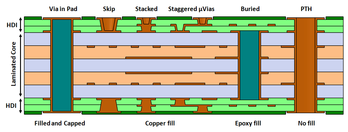
FIG. 1 - Types of PCB vias
FIG. 1 presents quite a complex 10 layer HDI construction PCB with different kinds of vias. Let's go over this as an introductory and explain different concepts and also review some terminology used in the PCB world. For this tutorial, let's assume FR-4 materials only, this means cores and prepregs which are based on woven glass and epoxy.

HDI PCB Construction

HDI stands for high density interconnect, this construction involves multiple stages of lamination under the heat press and usually also multiple stages of drilling and plating (whereas regular multilayer board usually involves only one stage each of lamination, drilling, and plating). As such, this is a costly process and usage of features like via types, their filling, plating, and layer to layer drilling - should all be done with great care and understanding of the fabrication steps. Basically, you pay for the processes required and your objective is to find the best fit construction for the application requirements.

For interesting HDI build pictures, please refer to [4].

Microvia

HDI goes hand in hand with the microvia which is a laser-drilled plated hole that usually spans two layers only. The microvia is smaller than the standard plated through via, or PTV for short. As a rule of thumb, a 20/10 mil PTV is four times more area consuming than a 10/4 mil microvia - therefore the potential of space savings on the top and bottom component layers is significant.

In addition, because the PTV is a multilayer constraint, on a high layer count board the PTV consumes a lot of board space - little on each of the layers of the stackup, while the microvia only consumes area on the two copper layers it designed on. The HDI construction secret powers are all about eliminating as many PTVs as possible and the freedom to move the remaining ones to more convenient locations.

Stacked and Staggered Microvias

Stacked microvias are microvias that are designed on top of each other. They allow an electrical connection spanning more than one dielectric layer and at the same time maintain the small size of the standard microvia (as opposed, for example, to a skip via that must increase in size). In this configuration, copper filling (or less common, via capping) is required for all the microvias of the stack except for the outermost via, the same as a building having structural columns on each floor, here the copper filing is used for electrical connection between the microvias in the stack.

Staggered microvias offer an alternative construction in which the microvias are designed next to each other, like a stairway. Essentially these vias are designed as simple one-layer microvias and there is no need for via filling which is a time consuming and costly process.

The staggered microvias are considered more cost effective to produce and more reliable [7] than stacked microvias, however, from a signal integrity perspective the stacked configuration is better because of shorter connection path has lower parasitic inductance and capacitance.

Skip Via

Also called skip microvia, this is a special type of microvia that is designed to skip one copper layer and is usually designed from the outer layers. In FIG. 1 there are skip via from L1 to L3 and from L10 to L8.

The skip via can potentially save one drilling and one plating operation in the HDI PCB construction (as compared to stacked and staggered constructions) - if designed correctly and in case no other elements in the board require them.

However, these vias must be made larger than standard one-layer microvias because the plating of this via is more difficult to produce. In an attempt to reduce the size of the skip via, the PC designer might want to lower the prepreg thicknesses of the involved layers (i.e 1-2 and 2-3 prepregs) but this causes an additional constraint not previously required. This, in turn, might cause problems with impedance matching of traces with a very close plane layer.

Lastly, many manufacturers might not be as skilled in this process and may opt to change the design and quote their price based on a stacked microvia construction. This means that you might not get the cost benefit from this construction but you still 'paid' for the bigger via size in your PCB design.

Laminated Core

HDI board starts its fabrication as an ordinary multilayer board, referring in the figure above to the central laminated core. In comparison, the production of a regular board (non-HDI) only includes some final stages compared to the laminated core, these are the solder mask, surface finish (i.e ENIG, HASL, OSP, etc), and silkscreen. So we can think of the laminated core as a regular board that is missing some final processes.

The Laminated core involves a single heat pressing stage of cores and prepregs. The core (also called C-stage laminate or CCL - copper-clad laminate) comes as a sheet of woven glass fibers fully cured in epoxy and having copper foils attached on both sides (usually). In the figure above there are 3 cores seen as gray purple sheets. the manufacturer will etch away copper from all cores on both sides except for the outer layers of the laminated core, which will be etched only after plating the buried vias since the outer layers are needed for conduction of current during the copper plating process of the vias.

The prepregs, also called B-stage laminate, are sheets of woven glass fibers partially cured in epoxy (hence the name B-stage, to represent that additional curing is necessary). In the figure above we have 2 prepreg layers in light brown in between the 3 core sheets. The entire structure is then heat pressed to form the laminated core and then drilled and plated.

Buried Via

The buried via is drilled into the laminated core and as its name suggests, it will be later covered by additional layers of the PCB (the sequential buildup). Because of this reason, the buried via will usually be filled with epoxy so that there will not be open holes that can suck material from additional layers in the build. The buried via is mechanically drilled and the construction and clearances applied to regular multilayer vias are the same for the buried via.

Sequential Buildup

In the figure above, two layers are added from each side of the laminated core. This is referred to as sequential build since they are heat pressed in two additional stages after the laminated core has been prepared. In the first stage, the two inner layers are pressed to the top and bottom of the laminated core and in the second stage, the two outer layers of the PCB are added. In between these stages, there may be additional drilling and plating, that is highly dependent on the HDI construction and the types of vias designed.

PTH - Plated Through Hole

There is some ambiguity with the term PTH as some regard this as a via and some as other through holes. The PTH can mean both because any hole which is plated and going through all the layers in the board is a PTH, for examples holes for fitting a connector pin in which the lead is inserted and soldered to the hole. Via can also be a PTH but in this case, it will be better termed PTV - plated through via, this resolves any ambiguity with naming. Please also note that the term PTH is often used with an emphasis on the hole being plated while in contrast, the term NPTH emphasizes that the hole is not plated.

Via in pad (IPC 4761 type 7)

Also called VIPPO, this is one of the most interesting technologies. As the name suggest this via is allowed to be placed directly under pads of components on the board and as such the pad shape is not always round. Regular PTV must not be located on component pads because there is a problem of solder that can flow down the via's barrel and weaken the joint with the component's lead. However, the via in pad is fully shut and so solder wicking down the barrel is not a problem.

Basically, the via in pad is a through hole via which had its hole filled with epoxy or other conductive paste, then excess material is scraped from the outer surfaces to flatten it, and finally, the openings on top and bottom are plated over with copper. It is a costly operation that can add up to 20% to the board cost - since it involves many additional fabrication processes.

By the way, this via has way too many names which all refer to the same structure - sometimes called VIPPO, short for Via In Pad Plated Over, sometimes called filled and capped via, the standardized IPC name is IPC-4761 type 7, and the street name in china factories is just 'resin hole' (we don't recommend using this name as it's ambiguous). If you decided to use this type of filling make sure the manufacturer understands your requirement since there are other via filling options like plugging and tenting - so please be accurate in the fab notes documentation. Second, once this structure is decided, to lower costs it is better to specify all your PTV as VIPPO and avoid separate sets of constructions because this can add even more fabrication steps.

PCB Via Structure

The most basic via (often called through hole via or PTV) is shown below. It is somewhat simplified for better understanding and showing only copper elements on a 6 layer PCB as an example.

In this example, a trace on the top layer L1 is connected to a trace on layer L3. The traces are not part of the via but are shown as a typical application. This via is used for routing a net (a logical connection defined in the schematics), however, another common use  is for power supply connections where the via directly connected to an internal plane (not shown).
pcb via with non functional pads removed
FIG. 2 - Basic T.H. Via with unused pads removed
The through hole via comprises:
1. Barrel - a hole is drilled through all layers in the PCB (hence the name through hole), the hole is plated with copper for electrical connection. The barrel has a cylindrical shape and generally is considered as a fragile structure since it is long (e.g 1.6mm for a standard thickness PCB) and thin in diameter which is controlled by the hole size. The ratio of the hole diameter D to the barrel length L is referred to as the aspect ratio and is a measure of the barrel strength.

2. Pads - the pad is a circular copper area designed to engage in the center of the barrel. Since the lamination process of the copper layers involves some errors, a circular pad is designed to encircle the barrel - theoretically at the center, but some tolerance is provided to accept registration errors between the layers and also to allow for errors when the barrel hole is drilled. Some of the pads can be optionally removed on certain layers as we will discuss below.

It is worth noting that since the pads have a hole in their center - they are often not referred to as circular pads but rather as annular rings encircling the hole. Annular rings and their importance is discussed here.

Unused pads
Unused pads (also referred to as non-functional pads) are pads that do not serve the purpose of electronic connection and may be removed or retained. In FIG 1 they were eliminated while in FIG 2 they are retained for comparison. It is worth noting that both structures are used today and both are OK although some tradeoffs exist as discussed here. In FIG 3 the pads on L2, L4, and L5 are retained although the electrical connection is only from L1 to L3. The top and bottom layers also serve an additional purpose - they are used for electroplating the via barrel with copper. The top and bottom pads are almost always preserved but technically aside from these the only pads that are mandatory are those that are designed to accept the electrical connection. Other layers can have optional pads which are called unused pads or non-functional pads.

Here we show 2 via structures that only differ in their unused pads (also called non-functional pads). It is worth noting that both structures are used today and both are OK. We will discuss this in detail later on but for now, let's disregard the unused pads.

pcb via with non functional pads
FIG. 3 - Basic T.H. Via with unused pads retained

Annular Ring and IPC requirements

The annular ring size is critical to the via's function. It is defined as the distance from the hole up to the pad's edge. The annular ring is another way to look at the pad as a ring around the plated hole instead of as a full circle. The annular ring provides tolerance for accepting a hole that is not perfectly drilled on the center. Inner layer's pads also provide for tolerance against misregistration of the copper layers in the stackup. Generally, the thicker the annular ring, the more tolerance the design has against manufacturing errors, however increasing the via size consumes board space that could have been used for other important things such as components placement, routing, and internal planes - so a balance should be carefully evaluated between the different requirements.

In the figure below we describe as an example one of the most popular vias - the 20/10mil via. This means the via hole is 10mil (250um) and the surrounding pad is 20mil (500um / 0.5mm), the annular ring is 5mil (125um) as seen in FIG 4.


pcb via 20/10mil
FIG. 4 - The 20/10mil Via
The IPC has defined acceptance criteria for the annular ring. There are 3 so-called end product classes: class 1 (general electronic products) is the most forgiving to manufacturing tolerances, class 2 (dedicated service electronic products) is in the middle while class 3 (high-reliability electronic products) is reserved for boards where failure or downtime of the product cannot be tolerated. In the following sections, we will explain the acceptance criteria of the different classes.
via with 90 degree breakout due to drill tolerance
FIG. 5 - 90 degree breakout - OK for class 2 for pads on all layers
FIG 5 shows a 90 degree breakout, which means the via hole protrudes the pad such that a quarter of the hole's perimeter exits the pad. Class 2 generally accepts this breakout, and smaller breakouts than this, both in external layers and internal layers - provided that the breakout is not in the interconnect area of the pad and the trace. If the breakout is located in the interconnect area, it should not decrease the effective thickness of the copper by more than 20% of the minimum conductor width which is either specified or derived. For example, assuming we're using 4mil traces in the board and this is our minimum copper feature, and additionally assuming we didn't explicitly specify anything else in our fab notes to the manufacturer, this means that down to 3.2mil (4mil x 0.8) local neckdown of the trace is allowed for class 2.

Class 1 generally accepts breakouts of up to 180 angles. In case of the hole falling in the interconnect area of the pad and the trace - up to 30% reduction of the minimum copper width of the circuit is allowed.

Class 3 does not allow breakouts whatsoever. On external layers, 2mil minimum must be maintained as seen in FIG 6. On internal layers, 1mil minimum must be maintained as seen in FIG 7. As above, this is provided that the hole is not located in the interconnect area of the pad and the trace, if it is - then there is an additional requirement that the hole causes no more than 20% reduction of the minimum copper width (as specified in the fab notes or implied from the Gerber files) in the interconnect area.

As a side note, it seems that the requirement for the annular ring in class 3 has been somewhat relaxed in internal layers compared to external layers, however, this is not the case as there is a difference in the measuring of the annular ring between layers. On external layers, the annular is measured from the inside of the plated hole while on internal layers the annular ring is measured from the outside of the plated hole. Since the copper plating of the hole is about 1mil for class 3 this means that effectively the same requirement exists on all layers, the difference lies in the different measuring definitions.
via with 2mil annular ring due to drill tolerance
FIG. 6 - 2mil annular ring - OK for class 3 on external layers
via with 1mil annular ring due to drill tolerance
FIG. 7 - 1mil annular ring - OK for class 3 on internal + external layers
An interesting question that comes to mind: is it possible to take a class 2 board design and ask the manufacturer to make it according to class 3 for best reliability? The short answer is no, this is because the process tolerance cannot dramatically improve and any breakouts (among other things) or even minimum annular ring violations will result in poor yield. To comply with class 3 we need annular rings about 3mil larger than we had in class 2 and this requires significant redesign (if even possible). It is worth noting however that one can improve the reliability of the board even without making design changes. For example, we can specify higher copper plating in the barrel e.g 25um (comply with class 3) instead of the standard 20um (comply with class 1 and 2), we can also specify a lower aspect ratio (which means stronger via barrel) by requesting a lower stackup thickness or we can epoxy fill and cap the via (VIPPO structure, type VII according to IPC-4761). There are more ideas on how to make an existing board design more reliable but the general principle is that a class 3 board has to be designed as such from the early stages of layout and not as an afterthought.

Key takeaway: IPC 6012 class 2 annular ring

  • Up to 90 degree breakouts are allowed on all layers
  • Reduction of copper in the trace to annular ring junction area must not exceed 20% of the minimum conductor width
  • In any case, at least 50um of conductor width must remain in the junction area
  • The minimum conductor width can be specified in the fab notes, else it will be derived from the production files
  • Generally speaking, annular ring width of 5mil (125um) or more is recommended for meeting class 2 requirements

Clearance and Tolerances

The through hole via imposes a multilayer constraint, this is one of the biggest drawbacks of the standard non-HDI technology. As an example, let's assume a 6 layer board where L1 needs to connect with L3. That via still passes through the 6 layers of the board although only 2 layers need an electrical connection. The rest of the layers in the stackup have to maintain clearance from the via barrel and pads. Sometimes it is useful to think about this clearance as an 'Anti Pad' - as if an imaginary pad of no copper is encircling the barrel. Of course, an anti pad cannot be regarded as a feature of the via since the anti pad does not exist on the board, however, the clearance or lack of copper around the barrel must be maintained with sufficient tolerance for all layers that do not require electrical connection to the via.

It is important to understand that the clearance required is always from the drilled hole and not from the via pads. A pad, if available on a specific layer, can have the standard clearance of copper to copper traces. For example, if your board is keeping 4mil minimum space between traces, 4mil can also be used as clearance from the via pad and the next copper feature on that layer. However, copper to copper clearance is not the main concern, as stated above it is the drill to copper that is very important for the yield of the board, this is because the drilling process is done by high-speed machines, and in addition, it is done only after lamination of the layers - so errors in the positioning of the pads on the different layers add up.
pcb via drill to copper clearance
FIG. 9 - Drill to Copper Clearance
Generally, the drill to copper clearance should be 8mil (200um) minimum measured from the outer edge of the barrel. Major contributing errors are:
1. Mechanical drill tolerance - 3mil
The manufacturer has to use a high-speed process to be cost-effective, so the drilling machine moves very fast - which adds to the drilling tolerance. Furthermore, the fabrication panels (containing the boards to be drilled) in high volume production are stacked on top of each other so that through holes are drilled at one shot to multiple panels. Any movement between the panels during the drilling process will contribute to the error. The manufacturer can do better if required but that would increase to cost due to machines that are run slower and/or panels that are not stacked.

2. Lamination registration tolerance - 3mil
The stackup is pressed under heat to cure the prepreg resins between the cores. The prepreg, also called B stage laminate, is only partially cured to allow processing at the factory while the cores, also called C stage laminate, already comes to the factory fully cured. When the stackup is pressed together under heat the prepreg softens until fully cooled and cured, therefore the layers can still slightly move in the process.

While the drill and registration tolerances are intuitive to understand, there are more tolerances required in the fabrication process. Therefore 8mil(200um) is a good rule of thumb to use for vias while laying out the board. Keep in mind though that during layout the drill you specify is the finished hole, i.e this the inner diameter of the barrel. The barrel plating is 20-25um depending on the class therefore you may want to specify 9mil (225um) during layout as finished via hole to copper.

It is sometimes useful to think of the clearance as an Antipad and let us illustrate the conversion calculation by referring to the 20/10mil via as an example. The antipad is not a physical feature of the via, actually, the antipad does not even exist. The antipad is the absence of any copper features in the vicinity of the barrel assuming they have different nets (i.e a nearby copper trace or plane that must not be shorted to the barrel). The antipad is therefore a circular, invisible circle formed around the barrel at each copper layer, you can witness it if you have a plane or polygon pour (of different nets) located around the via - it shows as a circular cutout around the barrel. So, going back to the 20/10mil via and let's assume we would like to have clearance of 9mil from the finished hole size (inside diameter) then our antipad would be 28mil - (10mil finished hole) + (9mil x 2 clearance). Additionally, if the via has a pad around the barrel at a specific layer then standard copper to copper clearance must also be maintained, in our example the pad is 20mil and the antipad is 28mil so an additional 4mil clearance on all sides is already maintained. Of course, if we would like more clearance we would need to use a larger antipad.

PCB Aspect Ratio and Via Plating

The barrel of a multilayer via refers to the hole that extends from one side of the PCB to the other, the hole is plated with copper to provide an electrical connection between the layers. According to IPC-6012, classes 1 and 2 require an average copper plating thickness of 20um or more, and no less than 18um in thin areas, while class 3 requires a 25um average thickness or more and not less than 20um in thin areas. The same holds for buried vias as well but not for microvias that don't have a barrel and have relaxed requirements regarding plating. Therefore microvias will be discussed in a dedicated section.

via barrel and aspect ratio illustration
FIG. 10 - The Aspect Ratio D/H
As seen in FIG 10, the aspect ratio refers to the diameter of the hole D divided by the thickness H of the PCB (which is equal to the barrel's length).

The aspect ratio is a measure that is important both to the designer and manufacturer of the board since it highlights key insights about the reliability, cost, and manufacturability of the board. First, the aspect ratio can tell us about the manufacturability of the via (as well as any PTH in the board) and reveal a potential concern for the plating strength of the barrel. To explain this we need to shortly explain the electrolytic plating process of the via.

How Are PCB Vias Plated?

  • The process starts after the PCB has been laminated in the heat press.
  • The PCB has its internal layers etched, however the copper on top and bottom layers is not etched just yet.
  • Through holes are then drilled, unplated and non-conductive at this stage.
  • All holes go through multiple cleaning processes to remove debris from the drilling stage.
  • A small amount of conductive carbon is placed on the inside of the holes to be plated, the carbon acts as a metal seed layer to allow subsequent copper to grow upon.
  • The top and bottom copper layers are connected to a voltage source and the whole panel is entered into an electrolyte bath that contains copper ions.
  • The whole panel acts as a conductor allowing current to flow from the bath to the panel. Any area that has exposed metal will be plated by receiving copper ions from the solution in the bath - including the via holes.
  • The via holes are now plated and the next step is to etch the copper on the top and bottom layers. A protective tin coating is placed over the via top and bottom pads (including the barrel), to protect them from the next etching stage.
So we can understand now why larger aspect ratio holes plate more easily. The chemical solution that contains the copper ions can flow into the inside of the hole more easily for bigger hole diameters. Similarly, longer barrels (i.e thicker PCBs) make it more difficult to plate the inside of the barrel. Regardless of the aspect ratio, the center of the barrel (about midway from the top and bottom) is always the most difficult area to plate because fewer copper ions reach there - so this area is more prone to failure for example by thermal cycling which will be discussed below.

As a rule of thumb, from 10mil hole diameter and above - the aspect ratio can be 1:10 but for 8mil or lower a smaller aspect ratio is required, which means also thinner PCB. The following summarizes the permissible aspect ratios:
1. 12mil (300um) finished hole - aspect ratio 1:10 - board thickness max 3mm
2. 10mil (250um) finished hole - aspect ratio 1:10 - board thickness max 2.5mm
3. 8mil (200um) finished hole - aspect ratio 1:8 - board thickness max 1.6mm
4. 6mil (150um) finished hole - aspect ratio 1:6.6 - board thickness max 1mm (advanced process only)

Barrel Cracks

The barrel is a weak structure because of its geometry and is prone to cracking under thermal cycling, a process also known as barrel fatigue. The main reasons for the fragility of the barrel are:
1. The barrel has a geometry of a long and narrow tube. Unless special treatment is applied, it will also be hollow.
2. The copper of the barrel expands under heat much less than the cores and prepregs around it, causing mechanical stress.
3. The plating of the tube is thin, about 20-25um of copper.
4. The barrel is electroplated with copper which is more fragile than the lamination copper.
pcb barrel crack illustration
FIG. 11 - Barrel crack due to CTE mismatch
To understand the failure mechanism we need to explain what happens to the PCB when it is heated - whether during assembly of components or from self-heating under normal operation. The PCB is a laminate structure of different materials and every material has its coefficient of thermal expansion or CTE for short. The CTE is a measurement of a natural property of all materials, they change their dimensions when heated and cooled, and except for special cases, the CTE is positive - meaning that the material is expanded under heat and shrinks while cooling (the most notable exception to this is water at 0-4 degrees which expand, but let's disregard special cases). CTE in the laminate industry is split in two, the X/Y plane or in-plane which refers to the plane of the laminate, and the Z-axis which is in the direction of the barrel - normal to the PCB. This is important because the FR-4 (both prepreg and cores) is a mixture of glass fibers and epoxy and the glass fibers greatly assist in constraining the epoxy from expanding in the X/Y plane. However, in the Z-axis there is no such constraint and the CTE of epoxy is very high compared to the rest. This is often referred to as CTE mismatch and the relative movement of different materials side by side causes internal stress which could lead to cracking of the barrel.

It should be noted that there is a distinction in CTE pre-Tg and post-Tg. Tg stands for glass transition temperature, this is the temperature that the material transition from hard and brittle phase into soft rubbery phase. At around Tg, the CTE receives a sharp knee and becomes significantly higher (about 4x) in the Z-axis while on the X/Y plane there is no significant change due to the restricting glass fibers. For typical numbers, let's look for example at the Isola FR406. This is a medium-high grade FR-4 material with a Tg of 170C. Z-axis pre-Tg CTE is 60 PPM/C while post-Tg CTE is 250 PPM/C. In the X/Y plane, the CTE is 13 PPM/C both pre and post-Tg. As can be seen, post-Tg of 250 is much more severe than pre-Tg of 60. This also implies that operations like solder reflow during assembly can be very hard on the barrel and cannot be done too many times.

To illustrate by example let's provide some common numbers. The copper in the barrel has a CTE of about 17-18 PPM/C - parts per million per degree Celsius. Let's assume a 1.6mm barrel length for a standard thickness PCB and a 50 degree Celsius increase during normal operation of the board, under these conditions 18 * 1.6mm * 50 / 1,000,000 equals 1.44 microns. The barrel has just expanded by 1.44 microns. What about the cores and prepregs around the laminate? let's assume 60 PPM/C same as the FR406 above - so were at 60 * 1.6mm * 50 / 1,000,000 which equals 4.8 microns. As can be seen, the copper expands by less than one-third of the FR-4 in this example and the CTE mismatch results in strong forces between the barrel and its surroundings.

For additional information regarding thermal cycling and barrel cracks, please refer to [3] and [6].

References

[1] Thermal Conductivity & Coefficient of Expansion chart at RFCafe
[2] Creating Documentation for Successful PCB Manufacturing at Altium
[3] Thermomechanical failures in PTVs - DOEEET
[4] HDI build pictures - Shipco
[5] Annular rings - Sierra Circuits
[6] Laminate CTE - Iconnect007
[7] Stacked and Staggered Microvias Reliability - Paul Reid
Text Link